- 您现在的位置:买卖IC网 > Sheet目录325 > FAN7888MX (Fairchild Semiconductor)IC GATE DRIVER HALF BRIDG 20SOIC
�� �
�
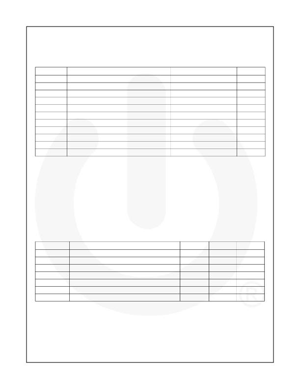
�Absolute� Maximum� Ratings�
�Stresses� exceeding� the� absolute� maximum� ratings� may� damage� the� device.� The� device� may� not� function� or� be� opera-�
�ble� above� the� recommended� operating� conditions� and� stressing� the� parts� to� these� levels� is� not� recommended.� In� addi-�
�tion,� extended� exposure� to� stresses� above� the� recommended� operating� conditions� may� affect� device� reliability.� The�
�absolute� maximum� ratings� are� stress� ratings� only.� T� A� =25°C,� unless� otherwise� specified.�
�Symbol�
�V� B�
�V� S�
�V� HO1,2,3�
�V� DD�
�V� LO1,2,3�
�V� IN�
�dV� S� /dt�
�Parameter�
�High-Side� Floating� Supply� Voltage� of� V� B1,2,3�
�High-Side� Floating� Supply� Offset� Voltage� of� V� S1,2,3�
�High-Side� Floating� Output� Voltage�
�Low-Side� and� Logic-fixed� Supply� Voltage�
�Low-Side� Output� Voltage�
�Logic� Input� Voltage� (HIN1,2,3� and� LIN1,2,3)�
�Allowable� Offset� Voltage� Slew� Rate�
�Min.�
�-0.3�
�V� B1,2,3� -25�
�V� S1,2,3� -0.3�
�-0.3�
�-0.3�
�-0.3�
�Max.�
�225.0�
�V� B1,2,3� +0.3�
�V� B1,2,3� +0.3�
�25.0�
�V� DD� +0.3�
�V� DD� +0.3�
�50�
�Unit�
�V�
�V�
�V�
�V�
�V�
�V�
�V/ns�
�P� D�
�Power�
�Dissipation� (1)(2)(3)�
�1.47�
�W�
�?� JA�
�T� J�
�Thermal� Resistance,� Junction-to-ambient�
�Junction� Temperature�
�85�
�+150�
�?� C/W�
�?� C�
�T� STG�
�Storage� Temperature�
�-55�
�+150�
�?� C�
�Notes:�
�1.� Mounted� on� 76.2� x� 114.3� x� 1.6� mm� PCB� (FR-4� glass� epoxy� material).�
�2.� Refer� to� the� following� standards:�
�JESD51-2:� Integral� circuits� thermal� test� method� environmental� conditions� -� natural� convection�
�JESD51-3:� Low� effective� thermal� conductivity� test� board� for� leaded� surface-mount� packages.�
�3.� Do� not� exceed� P� D� under� any� circumstances.�
�Recommended� Operating� Conditions�
�The� Recommended� Operating� Conditions� table� defines� the� conditions� for� actual� device� operation.� Recommended�
�operating� conditions� are� specified� to� ensure� optimal� performance� to� the� datasheet� specifications.� Fairchild� does� not�
�recommend� exceeding� them� or� designing� to� Absolute� Maximum� Ratings.�
�Symbol�
�V� B1,2,3�
�V� S1,2,3�
�V� DD�
�V� HO1,2,3�
�V� LO1,2,3�
�V� IN�
�T� A�
�Parameter�
�High-Side� Floating� Supply� Voltage�
�High-Side� Floating� Supply� Offset� Voltage�
�Supply� Voltage�
�High-Side� Output� Voltage�
�Low-Side� Output� Voltage�
�Logic� Input� Voltage� (HIN1,2,3� and� LIN1,2,3)�
�Ambient� Temperature�
�Min.�
�V� S1,2,3� +10�
�6-V� DD�
�10�
�V� S1,2,3�
�GND�
�GND�
�-40�
�Max.�
�V� S1,2,3� +20�
�200�
�20�
�V� B1,2,3�
�V� DD�
�V� DD�
�+125�
�Unit�
�V�
�V�
�V�
�V�
�V�
�V�
�°C�
�?� 2008� Fairchild� Semiconductor� Corporation�
�FAN7888� ?� Rev.1.0.1�
�4�
�www.fairchildsemi.com�
�发布紧急采购,3分钟左右您将得到回复。
相关PDF资料
FDA215S
IC DRIVER MOSFT DUAL PHOTO 8-SMD
FDS1212
SHELF FOLD DOWN 12X12" BEIGE
FDS1818
SHELF FOLD DOWN 18X18" BEIGE
FFSD-17-01-N
CONN SOCKET 34POS IDC .05"
FI-DP42CL1 PLUG
PLUG 42POS COAX DISCRETE WIRE
FI-J20C5-T3000
CONN PLUG 0.4MM 20POS
FI-X20C-NPB
CONN PLUG CABLE 1MM 20POS SOLDER
FIN4.00RD
FIREFLEX FIBERGLASS 4" RED 50'
相关代理商/技术参数
FAN7930
制造商:FAIRCHILD 制造商全称:Fairchild Semiconductor 功能描述:Interleaved Dual BCM PFC Controllers
FAN7930B
制造商:Fairchild Semiconductor Corporation 功能描述:
FAN7930BM
功能描述:功率因数校正 IC Critical Conduction Mode PFC Controller RoHS:否 制造商:Fairchild Semiconductor 开关频率:300 KHz 最大功率耗散: 最大工作温度:+ 125 C 安装风格:SMD/SMT 封装 / 箱体:SOIC-8 封装:Reel
FAN7930BMX
功能描述:功率因数校正 IC Critical Conduction Mode PFC Controller RoHS:否 制造商:Fairchild Semiconductor 开关频率:300 KHz 最大功率耗散: 最大工作温度:+ 125 C 安装风格:SMD/SMT 封装 / 箱体:SOIC-8 封装:Reel
FAN7930BMX_G
制造商:Fairchild Semiconductor Corporation 功能描述:IC PFC CTLR CRITICAL CONF 8-SOIC 制造商:Fairchild Semiconductor Corporation 功能描述:Power Factor Correction - PFC Critical Conduction Mode PFC Controller 制造商:Fairchild Semiconductor Corporation 功能描述:Critical Conduction Mode PFC Controller
FAN7930C
制造商:FAIRCHILD 制造商全称:Fairchild Semiconductor 功能描述:The FAN7930C is an active power factor correction(PFC) controller for boost PFC applications that operate in critical conduction mode(CRM).
FAN7930CM
功能描述:功率因数校正 IC Critical Conduction Mode PFC Controller RoHS:否 制造商:Fairchild Semiconductor 开关频率:300 KHz 最大功率耗散: 最大工作温度:+ 125 C 安装风格:SMD/SMT 封装 / 箱体:SOIC-8 封装:Reel
FAN7930CMX
功能描述:功率因数校正 IC Critical Conduction Mode PFC Controller RoHS:否 制造商:Fairchild Semiconductor 开关频率:300 KHz 最大功率耗散: 最大工作温度:+ 125 C 安装风格:SMD/SMT 封装 / 箱体:SOIC-8 封装:Reel